Description
Model 150-2D
Very High Resolution Reference and Traceable Standards for Magnification Calibration of AFM, SEM, Auger, and FIB General Purpose – High Precision A precision, holographic pattern provides accurate calibration in the horizontal plane for very high resolution, nanometer-scale measurements. Period:144 nm pitch, two-dimensional array. Accurate to ± 1 nm. Refer to calibration certificate for actual pitch. Surface: Aluminum bumps on Silicon, 4×3 mm die. Bump height (about 90 nm) and width (about 75 nm) are not calibrated.
 |
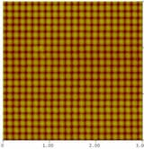
AFM Tapping Mode Scan The bump height is about 90 nm. This specimen is not recommended as a height reference because it is not easy for the standard AFM probes to reach the substrate level between the pumps. |
 |
For SEM, an independent analytical lab has tested this specimen in a FE-SEM (field emission scanning electron microscope). They found that the pattern was very uniform and the specimen was easy to image. No significant charging was observed in the voltage range 1-20 kV. Usability: the calibrated pattern covers the entire chip. There is sufficient usable area to make tens of thousands of measurements without reusing any areas altered or contaminated by previous scans
MODEL 150-2D:
This Calibration Reference specimen comes with a non-traceable, manufacturer’s certificate. These states the average period, based on batch measurements.
MODEL 150-2DUTC:
This traceable, Certified Standard is a select grade. Each standard is individually measured in comparison with a similar specimen calibrated at PTB. (PTB, Physikalisch-Technischen Bundesanstald, is the German counterpart of NIST). The uncertainty of single pitch value is typically ±1,4 nm (95% confidence interval). Multi-pitch measurements provide the usual square-root of N improvement in precision. Easy to use We recommended Model 150-2D because of its unique characteristics which make it especially easy to use. The specimen is durable and it allows you can scan in contact mode, offering you faster calibration and measurements. This is the only high resolution 2D calibration specimen we have seen that offers the following characteristics: – 2-dimensional array for simultaneous calibration of X and Y axes. – Pitch <500 nm. – Array of pumps mean the image contrast is high even when the probe tip is slightly dull. – High contrast in contact mode scans. – The pattern covers the entire die so that you don’t have to hunt for the scan area.The bump height is about 90 nm. This specimen is not recommended as a height reference because it is not easy for the standard AFM probes to reach the substrate level between the pumps. The bump height is about 90 nm. This specimen is not recommended as a height reference because it is not easy for the standard AFM probes to reach the substrate level between the pumps.
 |
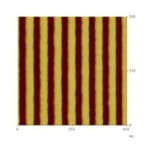
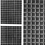
SEM High Magnification The following image was captured with a magnification setting of 100kX and accelerating voltage 10 kV |
 |
SEM Medium Magnification At 5 kX, the individual bumps were still well resolved. Large fields of view show how few defects are present. The most common defects are single missing bumps or a single extra bump inserted between lattice positions. Two vacancies are present in the image shown above. |

Reviews
There are no reviews yet.