Description
EM-Tec M-1 and M-10 Grid Pattern Calibration Standards
with 1um and 10um pitch grid patterns, NIST traceable
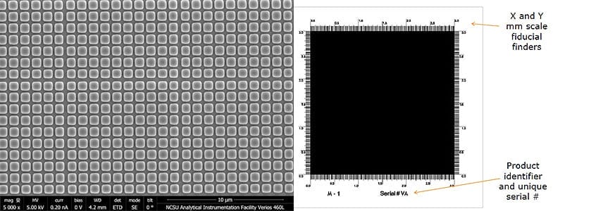
The EM-Tec M1 and M-10 calibration standards both have a square mesh type grid pattern etched in the surface of an ultra-flat Si substrate. The grid patterns are practical tools for magnification calibration and image distortion assessments. Intended for use with SEM, FESEM, FIB, Auger, SIMS and reflected light microscopy applications. The specimens can also be mounted directly on the pattern; in this case the pattern in the background will give a direct calibration within the image. This is especially useful when working with small samples and powders. The EM-Tec M1 and M-10 grid pattern calibration standards are supplied with a wafer level certificate of traceability to NIST.
There are two types of grid pattern calibration standards:
- EM-Tec M-1 with a 1µm pitch grid pattern for 100x to 10,000x magnification range
- EM-Tec M-10 with a 10um pitch grid pattern for 100x to 1000x magnification range
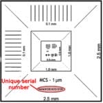
EM-Tec M-1 with 1µm pitch grid pattern for 100x to 10,000x magnification range
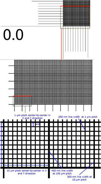 The EM-Tec M-1 has a grid pattern with a pitch of 1 µm and lines at 1, 10 and 100µm. Useful for calibration and image distortion checks in the 100x to 10,000x magnification range. Alternatively, the samples can be placed directly on the grid pattern for immediate calibration or internal calibration in the image. This is particularly useful for small samples. The lines are etched directly into the ultra flat Si substrate which will give superior signal strength compared to SiO2 etched structures.
Specifications for the EM-Tec M-1 calibration standard with 1 µm pitch grid pattern
| Substrate | 525µm thick boron doped ultra-flat wafer with <100> orientation |
| Conductive | Excellent; 5-10 Ohm resistivity |
| Pattern size | 3 x 3mm |
| Pitch/precision | 1µm ± 0.025µm, 10µm ± 0.025µm and 100µm ± 0.25µm |
| Line type / depth | Etched in Si, 300nm ± 30nm deep lines |
| Line width | 200nm ± 10nm for 1µm pitch lines 300nm ± 15nm for 10µm pitch lines 400nm ± 20nm for 100 µm pitch lines |
| Perpendicularity | Better than 0.01° |
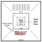
| Markers | Edge fiducial markers for grid position finding |
| Die size | 4 x 4mm |
| Application | SEM, FESEM, FIB, Auger, SIMS and reflected light microscopy |
| Identification | Product ID with serial number etched |
| Mounting | Unmounted, mounting optionally available |
| Supplied | Supplied in a Gel-Pak box |
| Certification | Wafer level certificate of traceability to NIST |
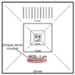
EM-Tec M-10 with 10µm pitch grid pattern for 100x to 1000x magnification range
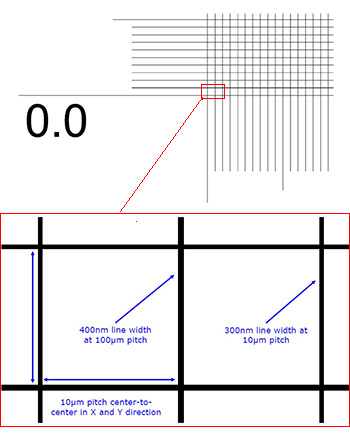
The EM-Tec M-10 has a grid pattern with a pitch of 10 µm and lines at 10 and 100µm. Useful for calibration and image distortion check in the 100x to 1000x magnification range. Samples can also be placed directly on the grid pattern for direct calibration or internal calibration in the image. This is practical for small samples. The lines are etched directly into the ultra flat Si substrate which will give superior signal compared to SiO2 etched structures.
Specifications for the EM-Tec M-10 calibration standard with 10 µm pitch grid pattern
| Substrate | 525µm thick boron doped ultra-flat wafer with <100> orientation |
| Conductive | Excellent; 5-10 Ohm resistivity |
| Pattern size | 3 x 3mm |
| Pitch/precision | 10µm ± 0.025µm and 100µm ± 0.25µm |
| Line type / depth | Etched in Si, 300nm ± 30nm deep lines |
| Line width | 300nm ± 15nm for 10µm pitch lines\
400nm ± 20nm for 100 µm pitch lines |
| Perpendicularity | Better than 0.01° |
| Markers | Edge fiducial markers for grid position finding |
| Die size | 4 x 4mm |
| Application | SEM, FESEM, FIB, Auger, SIMS and reflected light microscopy |
| Identification | Product ID with serial number etched |
| Mounting | Unmounted, mounting optionally available |
| Supplied | Supplied in a Gel-Pak box |
| Certification | Wafer level certificate of traceability to NIST |
Avis
Il n’y a pas encore d’avis.