

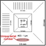
Description
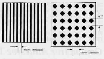
White area material: Tungsten.
Black area material: Tungsten, or other metal.
Materials: The calibration specimen consists of a silicon chip with a thin (100nm) thick polymer layer containing the pattern and a thin tungsten film over-coating the entire surface. The tungsten film varies from 20nm to 60nm in thicknenss, depending on the particular model. This structure has been proven under a wide varitey of beam conditions,
from 30kV to sub 12 kV.
Dimensions: 300nm or 700nm nominal (exact dimension will be provided with sample). Measurements are made from leading edge to leading edge, etc. Width of individual bars and spaces is not calibrated.
Background
EMS MXS « CE » and « BE » series SEM magnification reference gratings and grids set new standards for sub-micron accuracy and ease-of-use. Designed to meet the requirements for a reasonable cost, accurate sub-micron reference standard, « CE » Series Reference Standards can be tailored to meet a variety of needs.
They are ideal for student practice and instruction, testing new ideas or applications, or other uses where you need a good quality standard but do not want to put an expensive sample at risk.
Exceptional accuracy, repeatability, and uniformity are assured since each individual standard is an original or master produced directly from a holographic interference pattern.
These reference standards are remarkably durable under typical operating conditions. The surface contamination behavior is also very good. There are no better sub-micron reference standard available in this price range.
One test site indicated that on a scale of 1 to 5 with respect to ease of use, contrast/brightnes, durability, and accuracy, « CE » series reference standards earn a 4.7 out of 5 average in comparison to other available standards. Comments from various other test sites included « very good contrast/brightness levels at all voltages used, » « easy to use, » and « could become my secondary standard of choice. »
Application
EMS’s MXS « CE » series reference standards provide a calibrated dimension of either 300 nm or 700 nm nominal length. (« BE » series available only 300 nm)
The larger dimension provides accurate, multiple period measurement from about 5000X to over 45,000X while
the smaller dimension is useful from about 10,000X to over 100,000X.
Throughout this magnification range, these standards provide excellent image contrast, an enormous useful calibration area, and a 3-sigma accuracy of at worst 3%, with typical values around 1%.
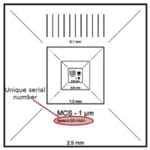
MXS « CE » and « BE » series reference standards are available as unmounted 3 mm x 4 mm pieces to be mounted by the microscopist, or pre-mounted for easy insertion in your SEM. Mounting one of these calibration standards is striaghtforward. The front surface of the sample and the silicon substrate are conductive. Experience indicates that there is, in general, no need to make a special effort to ground the front surface. The use of conductive silver or carbon-loaded paint, conductive epoxies, conductive tape, etc. have all been used to successfully mount « CE » Series standards.
With EMS’s MXS « CE » and « BE » Series Reference Standards, you can:
Quickly check dimensional measurements by mounting one on your specimen stage.
Perform periodic calibration and performance checks of your microscope.
Obtain high magnification, sub-micron-scale dimensional accuracy for the first time.
Accurately determine dimensions from 0.3 µm to 30 µm all with one calibration artifact.
Analyze your images for pin-cushion distortion, small-scale vibration, or small magnetic field distortions.
The accuracy of the « CE » Series Reference Standards, allows the microscopist to use them as a secondary standard. Their accuracy and uniformity make it easy to obtain and document traceability of measurements without placing an expensive, hard to obtain, difficult to use primary calibration standard at risk of contamination or damage.
Certification and Accuracy
MXS « CE » Series Reference Standards provide a calibrated dimension of either 300 nm or 700 nm nominal length. The actual dimension of the artifact as delivered will generally not be exactly these values. Both the fabrication process determines the actual dimension and by a second, independent measurement after the calibration artifact is manufactured.
The expected accuracy of the holographic technique used in the manufacturing process is ±0.1%. Unfortunately, subsequent processing steps degarde this initial accuracy, leading to the 3-sigma accuracy of 3% for the finished product. The second, independent measurement technique has an expected 3-sigma accuracy of 1% or better. Our experience is that the two measurement techniques applied to a particular artifact will agree with each other within 0.5mm.
It is important to remember that the certified dimension in an MXS « CE » and « BE » Series Reference Standard is not just at one unique position on the artifact, but is known at all locations on the standard.
Durability and Charging Effects
EMS MXS « CE » and « BE » Series Reference Standards have been tested and evaluated over a broad range of operating conditions, from those found in a tungsten filament system to the highest resolution FEG system. These standards have been found remarkably durable during use, with no beam-induced distortion in the calibrated pattern after as much as one-half hour of imaging time at 50,000X and 20 KV. Charging is minimal to non-existent, though edge-effect can be seen under some conditions. The high contrast and brightness, which can be obtained using these reference standards guarantees good contamination tolerance.
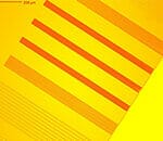
1. MXS 301CE and MXS 701CE
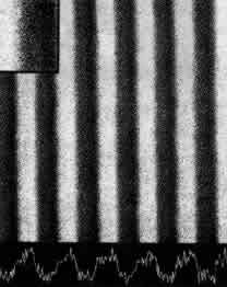
The calibrated dimension is the spatial period of a series of parallel ribs running across the surface of the sample. The significant height of the ribs (>100 nm) provides excellent image contrast. The top surface of the rib structures is somewhat rounded rather than completely flat. The edges of the ribs are readily discernible, with over 75% of the 3 mm by 4 mm sample area exhibiting an edge location variation, which is less.
Use and Imaging
The exceptionally clean and uniform pattern provided in an MXS 301CE or MXS 701CE standard displays few imperfections, which can be used as focusing and stigmation aids. For this reason, care roper stigmation is crucial since improper stigmation is not readily apparent when imaging a pattern of straight line. Once a proper focus and sigmation are obtained, the image can be shifted to an appropriate area and the desired measurements made.
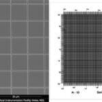
2. MXS 702CE
The calibrated dimension is the spatial period of a series of a 2-dimensional grid spread across the surface of the sample. This grid consists of a series of cylindrical posts rising from the surface of the sample. The significant height of the ribs (>100 nm) provides excellent image contrast. The top surface of these posts is somewhat rounded rather than flat and there are also slight departures from a perfect circle in the shape of some posts. Measurement techniques must be used which take these characteristics into account. The center-to-center distance of any pair is the most accurate measurements.
Use and Imaging
The exceptionally clean and uniform pattern provided in an MXS « CE » series 2-dimensional calibration standard displays few large scale imperfections which can be used as focusing and stigmation aids. For this reason, taking care in setting up the image before measurement is important. To assist in this process, an instruction sheet is provided with each standard. This sheet provides several example images which can be used to determine if the image of the sample is correctly set up.
The characteristics of the MXS 702CE standards make it easier to image than the 1-dimensional standards. The 2-dimensional grid facilitates setting the stigmation of the image properly. Once proper focus and sigmation are obtained, the image can be shifted to an appropriate area and the desired measurements made.Since the pattern covers the entire sample area, it is possible to make over 1,000,000 measurements utilizing the standard without using the same area twice.
Cleaning for the CE Series
Cleaning is possible using dry air or other clean gases, high purity distilled or deionized water, and soft brushes. Rubbing with soft tissues, or any other firm physical contact, or the use of solvents such as acetone or alcohol will damage the surface of the reference standard.
3. MXS 301BE
The calibrated dimension is the spatial period of alternating lines of Titanium and Silicon. The use of two different elements provides excellent image contrast, and the titanium layer thickness is kept to 20 nm to control edge distortion effects in the SEM image. These physical characteristics make the edges sharp and readily discernable. The calibrated pattern covers the entire sample, providing over 1,000,000 measurement sites. Because the pattern is a direct recording of a laser-generated interference pattern which has been transferred into the 20 nm thick Titanium film, these calibration samples are the most accurate available.
Imaging and Application
The exceptionally clean and uniform pattern provided in an EMS MXS « BE » series calibration standard displays few imperfections which can be used as focusing and stigmation aids. For this reason, care in setting up the image before measurement is important. To assist in this process, an instruction sheet is provided with each standard. This sheet provides several example images which can be used to determine if the image of the sample is correct. Once a proper focus and stigmation are obtained, the image can be shifted to an appropriate area and the desired measurements made.
The full screen image provided by an EMS calibration sample provides a unique advantage. Most calibration standards really verify accuracy of one portion of the image, while the entire screen is part of the measurement tool. With an image that fills the screen, you can quickly diagnose all types of image distortions, including problems due to vibrations, external fields, etc. A common problem is distortion caused by missadjusted CRT’s or scanners in which the magnification in one part of the image is different from another part of the image. Such problems are easily found and corrected using these calibration samples.
Cleaning for the BE Series
Titanium on Silicon produces a very durable calibration pattern. The calibration standard can be cleaned using common solvents such as acetone or alcohol, detergents, deionized water, etc. Gentle physical rubbing with soft tissues, brushes, etc., should not damage the sample. In extreme cases, cleaning by oxygen plasma may be possible.
Product Data
| 301CE & 701CE | 702CE | 301BE** | |
| Substrate | Silicon Wafer | Silicon Wafer | Silicon Wafer |
| Top Surface | 60 nm Tungsten film | 60 nm Tungsten film | Ti pattern on Si |
| Physical Size | 3mm x 4mm x 0.5mm | 3mm x 4mm x 0.5mm | 3mm x 4mm x 0.5mm |
| Accuracy | ± 3% | ± 3% | ± 3% |
| Nominal Dimensions | (x) | (x, y) | (x) |
| 300 nm for 301CE | 300 nm for 301BE | ||
| 700 nm for 701CE | 700 nm for 702CE | ||
| Availability | mounted or unmounted* | mounted or unmounted* | mounted or unmounted* |
*The cost for mounted samples using standard aluminum pin type stubs (EMS #75200). Please call us for additional expense.
**MXS-301BE Calibration sheet provided with standard contains actual dimensions to 3 significant figures. NPL tracability is also available with an additional cost.

Avis
Il n’y a pas encore d’avis.