25 résultats affichés
Filtres Trier les résultats
Rafraîchir Appliquer
L'échantillon de test KPFM & EFM a été spécialement conçu pour tester les performances de la microscopie à force à sonde Kelvin et de la microscopie à force électrostatique. Cet échantillon de test pratique est constitué de réseaux avec des lignes alternées d'aluminium et d'or déposées sur un substrat de silicium recouvert d'oxyde de silicium | |
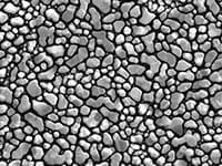
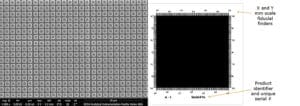
Gold on carbon resolution test standard with gold particles on a carbon substrate. The gold particles size ranges from 5-200nm. The carbon substrate is 6mm diameter with 2mm height. Gold provides excellent SE signal whereas the dark carbon background separates the individual gold particles. Feature rich gold particles are ideal for resolution testing on standard SEMs. Use with a magnification of 15,000x or higher. Ideally suited to correct distortion, astigmatism and image shift and to adjust for correct focus, beam size, contrast and brightness. This resolution standard has a square mesh grid pattern to facilitate locating and positioning.
Available unmounted or mounted on the most popular SEM stubs. If you work with multiple SEM platforms, look at our SEM stub adapter page. The SEM stub adapters enable you to use a single resolution standard on all SEMs. | |
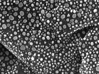
Gold on carbon resolution test standard with larger gold particles on a carbon substrate. The gold particles size ranges from 30-300nm. The carbon substrate is 6mm diameter with 2mm height. The larger gold particles provide excellent SE signal whereas the dark carbon background separates the individual gold particles. The feature rich larger gold particles are ideal for low kV and medium maginfication range. Use with a magnification of 10,000x or higher. Ideally suited to correct distortion, astigmatism and image shift and to adjust for correct focus, beam size, contrast and brightness. This resolution standard has a square mesh grid pattern to facilitate locating and positioning.
Available unmounted or mounted on the most popular SEM stubs. If you work with multiple SEM platforms, look at our SEM stub adapter page. The SEM stub adapters enable you to use a single resolution standard on all SEMs. | |
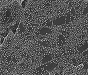
Gold on carbon resolution test standard with fine gold particles on a carbon substrate. The gold particles size ranges from 3-50nm. The carbon substrate is 6mm diameter with 2mm height. The fine gold provides excellent SE signal whereas the dark carbon background separates the individual gold particles. The finer gold particles are ideal for high resolution testing on standard SEMs and FESEMs. Use with a magnification of 50,000x or higher. Ideally suited to astigmatism and image shift and to adjust for correct focus, beam size, contrast and brightness for high resolution imaging. This resolution standard has a square mesh grid pattern to facilitate locating and positioning.
Available unmounted or mounted on the most popular SEM stubs. If you work with multiple SEM platforms, look at our SEM stub adapter page. The SEM stub adapters enable you to use a single resolution standard on all SEMs. | |
Gold on carbon resolution test standard with finer gold particles on a carbon substrate. The gold particles size ranges from 2-30nm. The carbon substrate is 6mm diameter with 2mm height. The finer gold provides excellent SE signal whereas the dark carbon background separates the individual gold particles. The finer gold particles are ideal for ultra high resolution testing on FESEMs. Use with a magnification of 100,000x or higher. Ideally suited to correct astigmatism and image shift and to adjust for correct focus, beam size, contrast and brightness for ultra high resolution imaging. This resolution standard has a square mesh grid pattern to facilitate locating and positioning.
Available unmounted or mounted on the most popular SEM stubs. If you work with multiple SEM platforms, look at our SEM stub adapter page. The SEM stub adapters enable you to use a single resolution standard on all SEMs. | |
EM-Tec M-1 with a 1µm pitch grid pattern is useful for calibration or image distortion asessments in the 100x to 10,000x magnification range. Pattern size is 3x3mm with lines directly etched in a conductive ultra-flat silicon substrate. Lines are 300nm deep with a width of 200nm for 1µm lines, 300nm for 10µm lines and 400nm for 100µm lines. Alternatively, small samples can be placed direction on the grid pattern for immediate calibration or integrated calibration in the image. This standard is NIST traceable; example of wafer level certificate of traceability for the Em-Tec M-1 grid pattern calibration standard.
Intended for SEM, FESEM, FIB, Auger, SIMS and reflected light microscopy | |
EM-Tec M-10 with a 10µm pitch grid pattern is useful for calibration or image distortion assessments in the 100x to 1000x magnification range. Pattern size is 3x3mm with lines directly etched in a conductive ultra-flat silicon substrate. Lines are 300nm deep with a width of 300nm for 10µm lines and 400nm for 100µm lines. Alternatively, small samples can be placed direction on the grid pattern for immediate calibration or integrated calibration in the image. This standard is NIST traceable; example of wafer level certificate of traceability for the Em-Tec M-10 grid pattern calibration standard.
Intended for SEM, table top SEM, FIB, Auger, SIMS and reflected light microscopy. | |
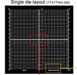
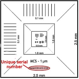
The EM-Tec MCS-0.1 calibration standard has been developed to accurately calibrate SEM, FESEM, FIB, Auger, SIMS and reflected light microscope systems. Suitable for magnifications from 10x to 200,000x. Bright chromium deposited features on ultra-flat conductive silicon for calibration down to 2.5µm and gold over chromium for 1µm to 100nm calibration features. The metal lines on silicon exhibit excellent signal with high contrast. The feature sizes for the MCS-0.1 are:
2.5mm, 1.0mm, 0.5mm, 250µm, 100µm, 10µm, 5µm, 2.5µm, 1µm, 500nm, 250nm and 100nm. The 31-T32000 EM-Tec MCS-0.1TR is NIST traceable on the wafer level against a NIST calibrated standard. Offered unmounted or mounted on the most popular SEM stubs. Good alternative for the discontinued SIRA calibration standard.
Example of wafer level certificate of traceability for the EM-Tec MCS-0.1TR magnification calibration standard, 2.5mm to 100nm. | |
The EM-Tec MCS-0.1-XY calibration standard has been developed to most accurately calibrate SEM, FESEM, FIB, Auger and SIMS systems. Suitable for magnifications from 10x to 200,000x. Brigth chromium deposited features on ultra-flat conductive silicon for calibration down to 2.5µm and gold over chromium for 1µm to 100nm calibration features in X and Y direction. The metal lines on silicon exhibit excellent signal with high contrast. The feature sizes for the MCS-0.1-XY are:
2.5mm, 1.0mm, 0.5mm, 250µm, 100µm, 10µm, 5µm, 2.5µm, 1µm, 500nm, 250nm and 100nm in X and Y direction. The 31-C32000 EM-Tec MCS-0.1CF-XY is individually certified utilizing a NIST calibrated standard. Offered unmounted or mounted on the most popular SEM stubs. Excellent alternative for the discontinued SIRA calibration standard with easier to use compatible feature sizes. |
