Description
Very High Resolution Calibration Reference and Traceable Standard for AFM, SEM, Auger, and FIB
For General Purpose and Metrology Microscopes
A precision pattern providing accurate calibration in the horizontal plane for very high resolution, nanometer-scale measurements.
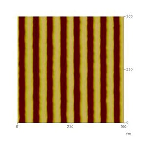
Period: 70 nm pitch, one-dimensional array. Accurate to +/- 0.25 nm. Refer to calibration certificate for actual pitch.
Surface: Silicon Oxide ridges on Silicon, 4×3 mm die. Ridge height (about 35 nm) and width (about 35 nm) are not calibrated.
For AFM, use in contact, intermittent contact (TappingMode™) and other modes with image sizes from 100 to 3000 nm. Available unmounted or mounted on steel disks.
For SEM, this specimen works well at a wide range of accelerating voltages (1 kV to 20 kV have been tested) and calibrates images from 25 kX to 1000 kX. Normally supplied unmounted. Can be mounted on a stub of your choice.
Usability: The calibrated pattern covers a 1.2×0.5 mm area. There is sufficient usable area to make thousands of measurements without reusing any areas altered or contaminated by previous scans.
Model 70-1D
This Calibration Reference specimen comes with a non-traceable, manufacturer’s certificate. This states the average period, based on batch measurements. This specimen is available only mounted on steel disk.
Model 70-1DUTC
This Traceable, Certified Standard is measured in comparison with a standard calibrated at PTB. (PTB, Physikalisch-Technischen Bundesanstalt, is the German counterpart of NIST. The standard is “NIST-Traceable” by virtue of the mutual recognition agreement between NIST and PTB.) The uncertainty of single pitch values is typically +/- 0.5 nm (95% confidence interval). Multi-pitch measurements provide the usual square-root of N improvement in precision.
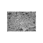
AFM Tapping Mode scan
For SEM, an independent analytical lab has tested this specimen in a FE-SEM (field emission scanning electron microscope). They found that the pattern was very uniform and the specimen was easy to image. No significant charging was observed in the voltage range 1-20 kV.
Usability: the calibrated pattern covers the entire chip. There is sufficient usable area to make tens of thousands of measurements without reusing any areas altered or contaminated by previous scans
The ridge height is about 35 nm. This specimen is not recommended as a height reference because the standard AFM probes may not always reach the substrate level between the ridges. Nevertheless, the image contrast is high, even when the probe tip is slightly dull. You can scan in contact mode, which means you can calibrate and measure faster.


Easy to find Patterned area
The patterned area is easy to find. The three rectangles shown in the sketch below are visible in reflected light, with either the unaided eye or an optical microscope. In a low magnification SEM image, the contrast is reversed. The central rectangle, which is the grating pattern, is relatively bright. The grating lines are parallel to the long side of the rectangle, as suggested by the high magnification SEM image.
 |
| Die and location of pattern within die |
 |
| Low magnification SEM image |
 |
| SEM High Magnification Image Magnification= 200 kX Voltage= 5 kV. |
Ordering for the Very High Calibration and Traceable Standard:
Available in the following ways: unmounted, 15mm steel disk(for AFM), SEM pin stub, or any other type of SEM stub.
Avis
Il n’y a pas encore d’avis.